3D Simulation of Fin Geometry Influence on Corner Effect in Multifin Dual and Tri-Gate SOI-Finfets
A N Moulai Khatir1*, A Guen-Bouazza1, B Bouazza1
1 Research Unit of Materials and Renewable Energies URMER, Abou Bekr Belkaid University, Tlemcen, Algeria.
*Corresponding Author
A N Moulai Khatir
Research Unit of Materials and Renewable Energies URMER,
Abou Bekr Belkaid University,
Tlemcen, Algeria.
E-mail: nassim.mkan@yahoo.fr
Article Type: Review Article
Received: October 15,2013; Accepted: October 15,2013; Published: October 28, 2013
Citation: A N Moulai Khatir, A Guen-Bouazza, B Bouazza. (2013). 3D Simulation of Fin Geometry Influence on Corner Effect in Multifin Dual and Tri-Gate SOI-Finfets, Int J Nano Stud Technol, 02(04), 29-32. doi: dx.doi.org/10.19070/2167-8685-130006
Copyright: A N Moulai Khatir© 2013 This is an open-access article distributed under the terms of the Creative Commons Attribution License, which permits unrestricted use, distribution and reproduction in any medium, provided the original author and source are credited.
Abstract
In this work the corner effect sensitivity to fin geometry variation in multifin dual and tri-gate SOI-FinFETs is studied through a commercial, three-dimensional numerical simulator ATLAS from Silvaco International [1].
These devices are compatible with conventional silicon integrated circuit processing, but offer superior performance as the device is scaled into the nanometer range. This study aims wider to use multiple fins between the source and drain regions. The results indicate that for both multifin double and triple gate FinFETs, the corner effect does not lead to an additional leakage current and therefore does not deteriorate the SOI-FinFET performance.
2.Introduction
3.Device Geometry
4. Process and Device Simulation
5. Evaluation of Buccal Films of Nitrendipine
6.Simulation Results
7.Conclusion
8.Acknowledgement
9.References
Key Words
FinFET; SOI; SOI-FinFET; Corner effect; Double gate; triple gate FinFET; multifin FinFET.
Introduction
The silicon-on-insulator (SOI) fin field effect transistor (FinFET) is known as the fully depleted leanchannel transistor with a silicon film standing vertically [2]. With the continuous scaling of MOS devices, nonplanar double and tri-gate SOI-FinFET have become attractive for their good control of short-channel effects, ideal subthreshold slope, and high current drive [3],[4]. In the double gate SOI-FinFET, the gate wraps around the rectangular silicon fin from two sides because the upper part of the gate electrode is separated from the gate oxide by an additional nitride layer of 10 nm thickness. While for the triple gate SOI-FinFET the gate wraps around the rectangular silicon fin from three sides. However, to improve the power gain and current drive, we can multiply the number of fin to get a multifin SOI-FinFET. Most research work on multifin MOS devices have focused on their advantages in digital or switching applications. Their performance sensitivity with fin geometry is not well studied.
The task of this work is to investigate the influence on the fin geometry on the corner effect and the role of this effect on the electrical performance of SOIFinFET transistors.
Fig. 1 shows the structure of a tri-gate three-fin SOIFinFET, where Sfin denotes the fin spacing between two neighboring silicon fins. Wfin and Hfin are the fin width and fin height, respectively. Tmask represents the hard mask thickness on top of a silicon fin. Tpoly is the geometrical thickness of gate material on top of the hard mask and Tox is the thickness of gate oxide.
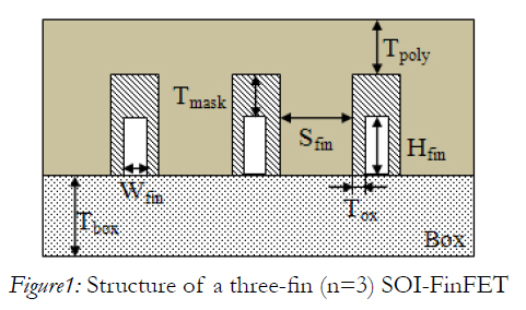
Figure1: Structure of a three-fin (n=3) SOI-FinFET.
Device Geometry
Two device geometries have been considered in this work: the gate wrap around triple gate SOI-FinFET transistor and the dual-gate SOI-FinFET transistor in which the gate wraps around the rectangular silicon fin from two sides.
The geometrical shape of the simulated three-fin dual and tri-gate SOI-FinFET structures are depicted in Fig.2 a and b. The three-fin triple gate SOI-FinFET shown in Fig.2-b consists of the silicon substrate, buried oxide isolation, the silicon fin, and the gate electrode. The gate oxide and other isolation and contact materials are not shown in this figure for clarity. The three-fin double gate SOI-FinFET in Fig.2-a differs from the triple gate transistor by the upper part of the active area which is not wrapped by the gate electrode.
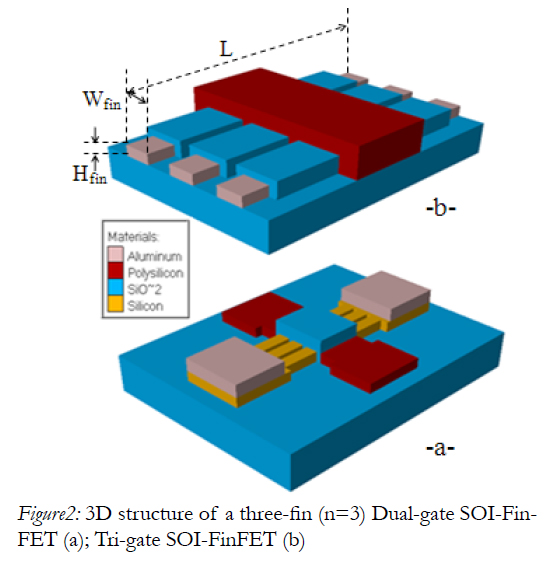
Figure2: 3D structure of a three-fin (n=3) Dual-gate SOI-Fin-FET (a); Tri-gate SOI-FinFET (b).
Because of the proximity of two adjacent gates in corners we get premature inversion [5]. The presence of charge sharing effect between two adjacent gates causes the premature inversion in the corners. The corners present gives rise to the formation of independent channels with different threshold voltages. This phenomenon is known as corner effect (Fig. 3).
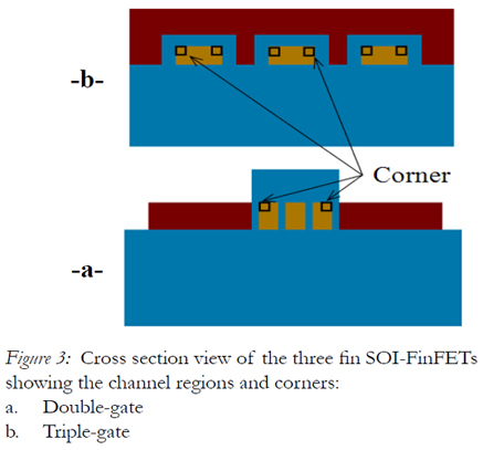
Figure 3: Cross section view of the three fin SOI-FinFETs.
showing the channel regions and corners:
a. Double-gate
b. Triple-gate
Process and Device Simulation
The 3D SILVACO simulation suite including, DevEdit3D and TonyPlot3D is performed in this article, in order to validate the basic principles and to uncover several important aspects: evaluation of the width and fin height effects on corner effects in three-fin double and tri-gate SOI-FinFETs. For this purpose each and one parameter was varied to study its effect independently of the others. The solution to remove the effects of the corner is proposed in [5]. If the doping of silicon is very weak or intrinsic, the corner effects are generally negligible; another solution is to round the corner. This is why the GAA does not have corner effects [6].
To neglect these corner effects we will try to minimize the part of corners compared to the all silicon film by increasing sufficiently the fin height (Hfin).
We adopted the drift-diffusion transport model in this study, partly because the ATLAS does not support advanced transport models in 3-D device simulation and because the drift-diffusion model mostly accounts for the salient features of the scaling properties. Physical gate length (LG) is 25 nm. The p-type body concentration is 1×1019 cm-3. The fin width is fixed at 50 nm, and the fin height is increased from 20 to 80nm.
Simulation Results
According to a comparison of the potential in the oxide and the silicon in the section perpendicular to the flow of the current for various heights of fin simulated with the simulator of the device Atlas of Silvaco shown in case of the three fin tri-gate SOI-FinFET (fig.4) and three fin dual-gate SOI-FinFET (fig.5) we see that for a high fin Hfin = 80 nm, the potential in silicon for both dual and tri-gate is nearly identical in the vertical direction. There is only one small portion of the potential which is not identical in the vertical direction near to the interfaces between the silicon and the gate above silicon and oxide of the substrate and which is smaller in tri-gate SOI-FinFETs because this last result from the penetration of the influences of side gates through oxide above the silicon and oxide of substrate.
When the fin height decreases until 50nm in three fin tri-gate SOI-FinFETs, if the fin width is sufficiently small; the potential in the vertical direction is still nearly identical.
The parts of the potential which are not identical in the vertical direction are neglected compared to the part of identical potential thanks to the good control of the transverse gates. While for the three fin dual gate SOI-FinFETs and because the gate above silicon has not an influence on the silicon compared to the side gates, this part of the potential not identical is larger. When the fin height is very small (Hfin=20nm),we cannot any more consider that the potential is identical in the vertical direction whatever the value of Wfin for the two cases.
The three fin tri-gate SOI-FinFET appears to be more advantageous in its electrical performance because no leakage current enhancement in the corners of the fin is observed. In contrast, we see a depletion of the leakage current in the upper corners of fin. The physical reason for this is the penetration of the negative electrical potential from the gate electrode into the corners and the penetration of the positive potential from the drain through the middle of the fin.
The corner effect at negative gate voltages results in a penetration of the negative surface potential into the active silicon and the consequence is the reverse corner effect, this means the depletion of the leakage current in the corners. The current density is mainly concentrated close to the surface and drops down rapidly. The enhancement of the current due to corner effect extends only over a very small region near the corner. This is due to a short screening length inside of inversion layer. The major effect in the double gate transistor is the suppression of the current near the upper surface of the fin, the on-current of the double gate transistors is higher than a simple estimation of 2/3 of the current of the triple gate transistors. In fact, the upper part of the fin also contributes to the total current of the open double gate transistor. A slight enhancement of the current in the corners of the fin in the open transistors is observed for both transistors.
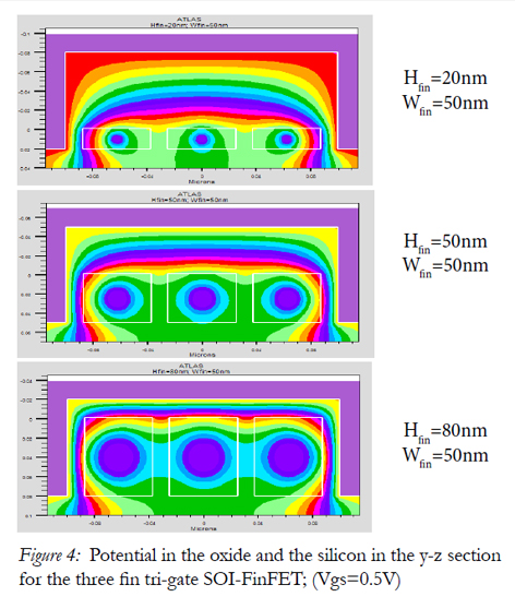
Figure 4: Potential in the oxide and the silicon in the y-z section for the three fin tri-gate SOI-FinFET; (Vgs=0.5V).
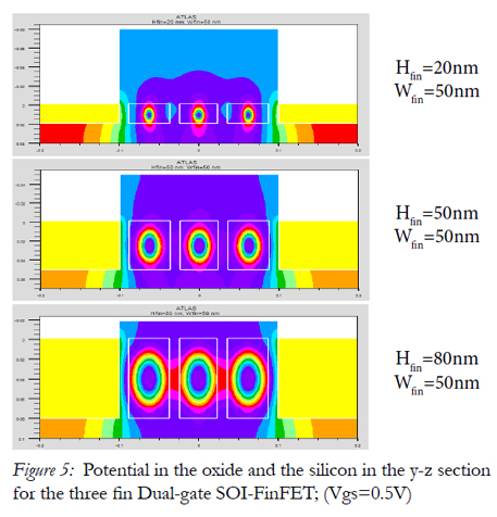
Figure 5: Potential in the oxide and the silicon in the y-z section for the three fin Dual-gate SOI-FinFET; (Vgs=0.5V).
Conclusion
The 3D structure of SOI-FinFET introduces new undesirable effects like the corner effect which can be well eliminated by a very weak doping of silicon or by an intrinsic silicon. In this work a study of the influence of fin geometry on corner effects in three fin Dual and Tri-gate SOI-FinFETs performances has been reported to present a new solution which will allow to eliminate this undesirable effect. [7],[8].
The corner effect improves the performance of the SOI-FinFETs since the on-current is enhanced at the corners and the leakage current is suppressed. Due to positive influence of the corner effect, the multifin triple gate wrap around design of the SOI-FinFET appears to be more advantageous in comparison to the multifin dual-gate design.
Acknowledgement
This work has been supported by the Research Unit of Materials and Renewable Energies URMER, Abou Bekr Belkaid University, Tlemcen 13000.
References
- ATLAS, Silvaco International, Santa Clara, CA, 2001.
- D. Hisamoto, T. Kaga, Y. Kawamoto, and E. Takeda, “A fully depleted lean-channel transistor (DELTA) - A novel vertical ultra thin SOI-MOSFET,” in IEDM. Tech. Dig, Dec. 1989,pp. 833–836.
- B. Yu, L. Chang, S. Ahmed, H. Wang, S. Bell, C.-Y. Yang, C. Tabery, C. Ho, Q. Xiang, T.-J. King, J. Bokor, C. Hu, M.-R. Lin, and D. Kyser, “FinFET scaling to 10 nm gate length,” in IEDM. Tech. Dig., Dec. 2002, pp. 25–254.
- J.-W. Yang and J. G. Fossum, “On the feasibility of nanoscale triple-gate CMOS transistors,” IEEE Trans. Electron Devices, vol. 52, no. 6, pp. 1159–1164, Jun. 2005.
- J. G. Fossum, J. W. Yang and V. P. Trivedi, “Suppression of Corner Effects in Triple-Gate MOSFETs”, IEEE Electron Device Letters, vol. 24, pp. 745-747, Dec 2003.
- M. Stadele, R.J. Luyken, M. Specht, W. Rosner, L. Dreeskornfeld, J. Hartwich, F. Hofmann, J. Kretz, E .Landgraf and L. Risch, “A comprehensive study of corner effects in tri-gate transistors” Proc; Solid-State Device Research Conférence (ESSDERC), pp 165-168, Leuven, Belgium, Sep. 2004.
- S. L. Tripathi, R.A. Mishra, “Performance improvement of FinFET using spacer high K dielectric”, J. Eectron Devices 17, 1447-1451(2013).
- Suman Lata Tripathi and R. A. Mishra, “Design of 20 nm FinFETs structure with Round Fin Corners including side surface slope variation”,J. Eectron Devices, 18, 1537-1642 (2013).